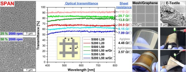
We present a solution-processable Ag nanostructure (SPAN) fabrication protocol for thin metallic nanoarchitectures exhibiting tunable optical and electrical properties as well as strong adhesion to general materials, including transparent, flexible, and fabric substrates and graphene-coated surfaces. The SPAN film can be fabricated in a scalable, vacuum-free fashion simply by the coating of an ionic Ag ink with a subsequent thermal annealing process. Here, we systematically analyze and confirm that the Ag nanoclusters are reduced from Ag ions and evolve into the nanostructured film, where its morphology and porosity as well as its optical and electrical properties can be readily controlled by adjusting the initial Ag ink concentration and coating speed as well as the annealing temperature. Compared to the conventional vacuum-deposited Ag layer, the SPAN film shows generally improved adhesion regardless of the substrate material with the aid of additional organic binding. The SPAN architecture can thus be applied to further scalable and pragmatic frameworks such as the transparent and flexible conducting electrodes consisting of micromesh-patterned SPAN structures on transparent, flexible, and/or graphene-coated substrates and SPAN-interwoven electronic textiles. Many diverse material systems and functional architectures can benefit from SPAN, including but not limited to smart sensors, plasmonic structures, and printable and wearable devices.
